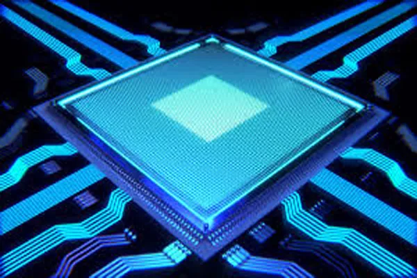
NVIDIA is known for creating some of the world’s most powerful chips, used in AI, gaming, data centers, and supercomputers. Building these “super chips” involves a combination of advanced design, manufacturing, packaging, and software optimization. Here’s how NVIDIA does it:
1. Advanced Chip Architecture
NVIDIA starts with its custom-designed architecture such as:
-
CUDA cores for parallel processing
-
Tensor Cores for AI acceleration
-
Ray Tracing Cores for graphics
-
High-speed interconnects like NVLink
These architectures are planned using billions of transistors and optimized for high performance and efficiency.
2. Collaboration With World-Class Foundries
NVIDIA does not manufacture chips itself.
They design the chips and partner with semiconductor fabs like:
-
TSMC (Taiwan Semiconductor Manufacturing Company)
-
Samsung (for earlier models)
These fabs use cutting-edge processes such as 5nm and 3nm lithography, enabling extremely small and efficient transistors.
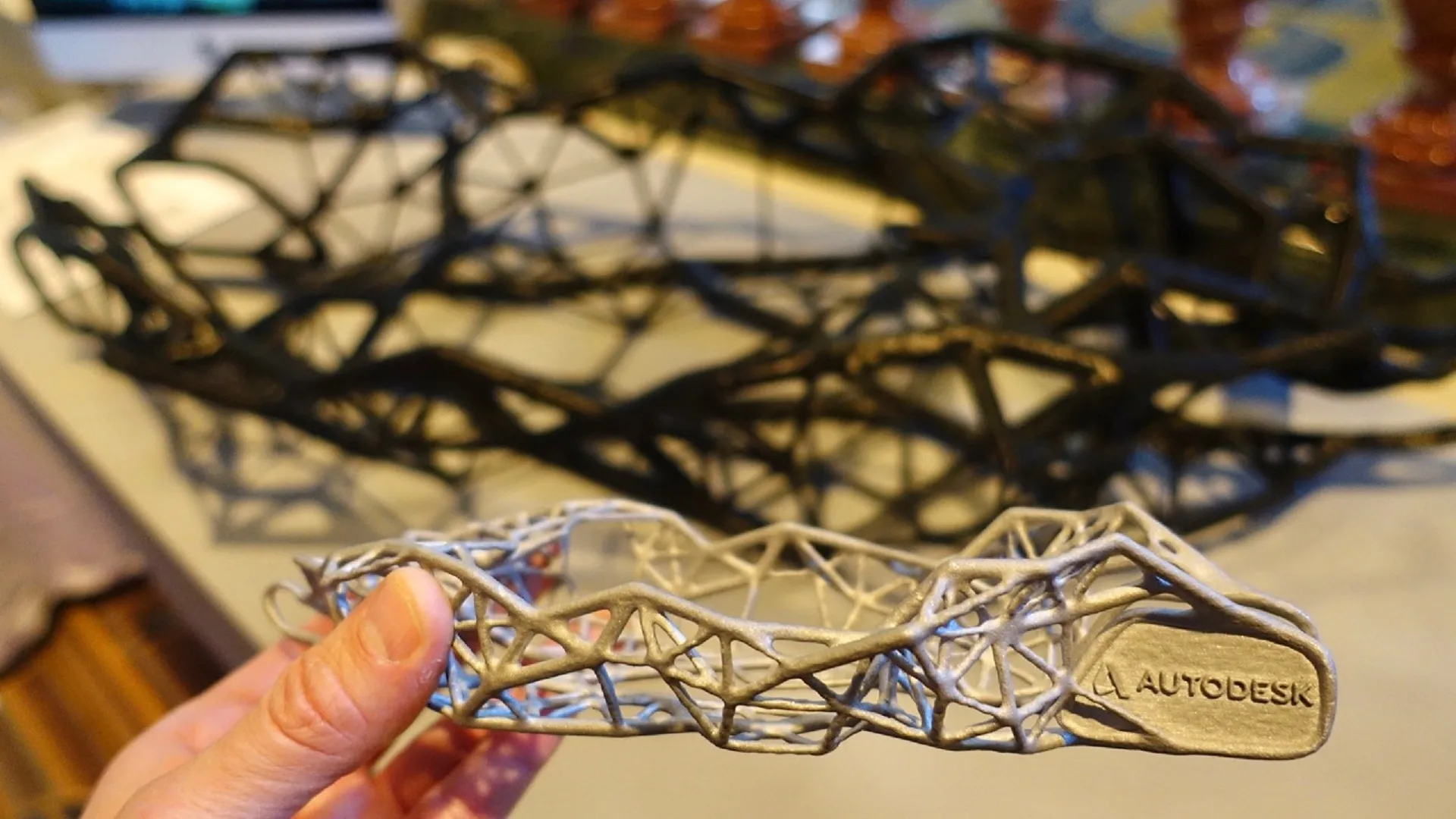
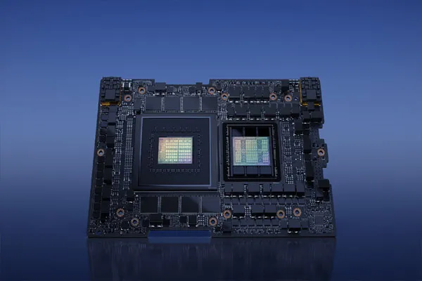
3. Multi-Die and Chiplet Technology
Modern super chips like NVIDIA Grace Hopper use:
-
Chiplets (multiple dies combined)
-
Advanced packaging like TSMC CoWoS (Chip-on-Wafer-on-Substrate)
This allows:
-
More cores
-
More memory bandwidth
-
Lower power consumption
-
Higher scalability
This is similar to stacking and linking multiple powerful chips into one unit.
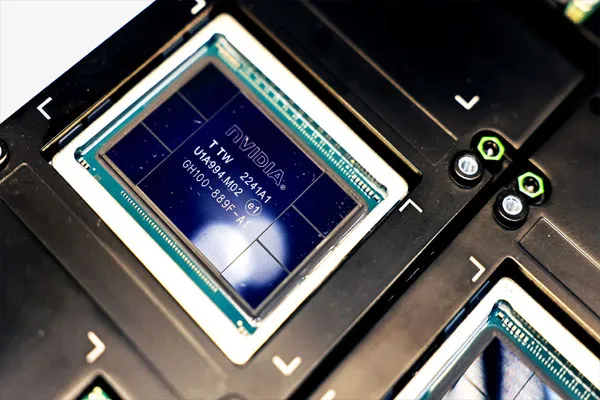
4. High-Bandwidth Memory (HBM) Integration
NVIDIA integrates HBM3 / HBM3e, a type of extremely fast memory placed very close to the processor.
Benefits:
-
Higher bandwidth for AI workloads
-
Lower latency
-
Improved energy efficiency
HBM is attached directly using 3D packaging technology.
5. Custom Interconnects for Faster Communication
NVIDIA super chips use:
-
NVLink for GPU-to-GPU communication
-
CCIX / PCIe Gen5 for CPU-GPU communication
-
NVSwitch for connecting multiple GPUs in a server
This creates an ultra-fast data transfer network, essential for AI training and supercomputing.
6. Extensive Software Ecosystem
Hardware is only half of the product. NVIDIA builds super chips along with:
-
CUDA (Parallel computing platform)
-
TensorRT, cuDNN (AI optimization libraries)
-
NVIDIA AI Enterprise
-
Driver & firmware frameworks
This software stack allows developers to unlock the full performance of their chips.
7. Testing & Validation
Before shipping, each super chip undergoes:
-
Thermal testing
-
Power efficiency tests
-
AI workload benchmarking
-
Reliability and stress testing
Only the highest-quality chips are selected for data centers.
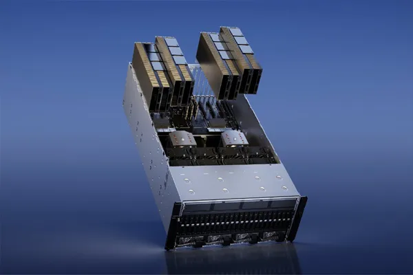
8. Integration Into Supercomputers
Finally, these chips are used to build:
-
AI servers
-
GPU clusters
-
Cloud compute platforms
-
National supercomputers
Systems like NVIDIA DGX and HGX combine multiple super chips to deliver world-leading performance.
Summary
NVIDIA builds super chips by combining:
-
Advanced architecture
-
Cutting-edge manufacturing (TSMC)
-
Chiplet + 3D packaging
-
High-bandwidth memory
-
High-speed interconnects
-
Powerful software ecosystems
This combination enables them to create some of the fastest computing chips in the world.